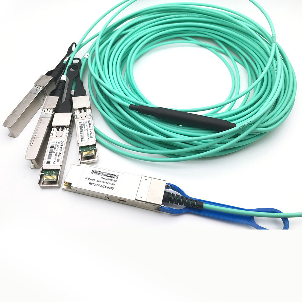
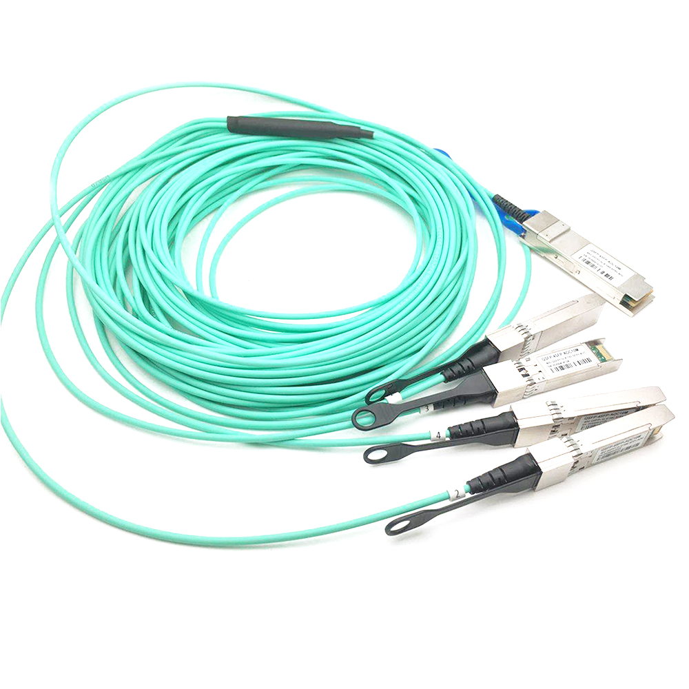
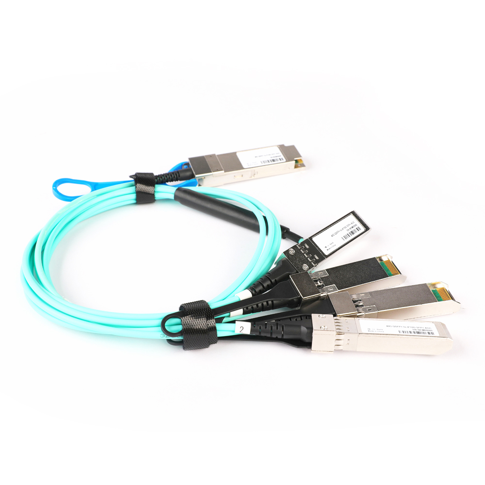
40Gbps QSFP+ to 4*SFP+ Active Optical Cable
Description
The active optical cables (AOC) that allows bi-directional 40Gbps to 10Gbps transmission suitable for high performance computing(HPC)clustering and other high-throughput data network, with advantages such as high speed, high density, low latency, low power consumption and light weight.
Features
> QSFP+ to 4*SFP+ module
> QSFP+ Maximum Aggregate Data Rate 40Gbps
> 4*SFP+ Maximum Aggregate Data Rate 4*10Gbps
> QDR,DDR,SDR(Infiniband)
> Bi-directional pararell link
> 10Gb/s per lane,X4 channels
> Up to 100m
> Low profile connectors
> Low power consumption
> Bundle multi-mode fiber array
> 850nm VCSEL four array
> PIN diode four array
> Hot-Pluggable
> I2C management interface
> From 0 to 70 degree case temperature
> 3.3V power supply voltage
> Electrical 38-pin connector
Standard
> Compliant with IEEE 802.3ba-2010,Annex 86A for 40GBASE-SR4
> Compliant with QSFP MSA(SFF-8436)
> Compliant with SFP MSA(SFF-8431)
> RoHS Compliant:lead-free
Applications
> Low-latency and high-speed interconnections for high performance computing(HPC)
> 40G Ethernet SR4
> Other high-throughput data transmission network
> Storage area Network(SAN)
Performance Specifications
Absolute Maximum Ratings
These values represent the damage threshold of the module. Stress in excess of any of the individual Absolute Maximum Ratings can cause immediate catastrophic damage to the module even if all other parameters are within Recommended Operating Conditions.
Table.1 Absolute maximum ratings
Parameter | Conditions | Min | Max | Units |
Power supply voltage at 3.3V | -0.3 | 4.5 | V | |
Voltage on I/O pads | -0.3 | VDD+0.3 | V | |
Differential Input Swing | 1.5 | Vpp | ||
Storage temperature | Non-condensing | -40 | 85 | Celsius |
Powered case temperature range | Non-condensing | -5 | 70 | Celsius |
Relative Humidity | 5 | 85 | % | |
Static discharge voltage onhigh speed pins | Human body model | 500 | V | |
Static discharge voltage on other pins | Human body model | 2000 | V | |
Air discharge to QSFP case | EN61000-4-2 Criterion B Test | 15 | kV | |
Contact discharge to QSFP case | EN61000-4-2 Criterion B Test | 8 | kV |
Recommended Operating Conditions
Table.2 Recommended Operating Conditions
Parameter | Conditions | Min | Typ. | Max | Units |
Data rate per lane | 8B/10BCoding, 64B/66B Coding | 1 | 10.3125 | 10.5 | Gbps |
3.3V Supply Voltage | 3.13 | 3.3 | 3.47 | V | |
Power supply noise including ripples | 1kHz to frequency of operation mersured at VCC_HOST | 50 | mVpp | ||
Case temperature | 0 | 35 | 70 | Celsius |
Transmitter Specification (Electrical)
Table.3 QSFP Transceiver Specification (Electrical)
Parameter | Condition | Min | Typ. | Max | Units |
Power Consumption | - | - | 0.8 | 1 | W |
Supply Current | - | - | 0.24 | 0.29 | mA |
Table.4 QSFP Transmitter Specification (Electrical)
Parameter | Test Point | Min | Max. | Units | Conditions |
Single ended input voltage tolerance | TP1a | -0.3 | 4 | V | Referred to TP1 signal common(Internally AC coupled) |
Differential input voltage swing | TP1a | 200 | 1600 | mVpp | Peak to peak differential |
AC common-mode input voltage tolerance | TP1a | 15 | - | mV | RMS |
Differential input return loss | TP1 | See IEEE 802.3ba 86A.4.1.1 | - | dB | 10MHz to 11.1GHz |
Differential to common-mode input return loss | TP1 | 10 | - | dB | 10MHz to 11.1GHz |
J2 jitter tolerance | TP1a | 0.17 | - | UI | |
J9 jitter tolerance | TP1a | 0.29 | - | UI | |
Data Dependent Pulse Width Shrinkage (DDPWS) tolerance | TP1a | 0.07 | - | UI | |
Eye mask coordinates: X1, X2 Y1, Y2 | TP1a | Specification values 0.11, 0.31 95, 350 | UI mV | Hit ratio = 5 x 10⁻⁵ see Figure. 3(a) |

a) Transmitter electrical input eye mask (b) Receiver electrical output eye mask
Figure 1. Eye Mask
Receiver Specification(Electrical)
Table.5 Receiver Specification (Electrical)
Parameter | Test Point | Min | Typ | Max. | Units | Conditions | |
Single ended input voltage tolerance | TP4 | -0.3 | - | 4 | V | Referred to signal common (Internally AC coupled) | |
AC common-mode input voltage | TP4 | - | - | 7.5 | mV | RMS | |
Differential Output swing (p-p) | TP4 | - | 320 (range 0) | - | mV | See details in the section “Memory Map”, page03, byte 238-239. | |
- | 420 (range 1) | - | mV | Default setting | |||
- | 740 (range2) | - | mV | ||||
- | - | 50 | mV | Squelched state | |||
Termination mismatch at 1MHz | TP4 | - | - | 5 | % | ||
Differential output return loss | TP4 | See IEEE 802.3ba 86A.4.2.1 | - | dB | 10MHz to 11.1GHz | ||
Common-mode output return Loss | TP4 | See IEEE 802.3ba 86A.4.2.2 | - | - | dB | 10MHz to 11.1GHz | |
Output transition time, 20% to 80% | TP4 | 28 | - | - | ps | ||
J2 jitter output | TP4 | - | - | 0.42 | UI | ||
J9 jitter output | TP4 | - | - | 0.65 | UI | ||
Eye mask coordinates: X1, X2 YI,Y2 | TP4 | Specification values 0.29, 0.5 150, 425 | UI mV | Hit ratio = 5 x 10⁻⁵ see Figure. 3(b) | |||
Test Point Definition

Figure 2. Test Point
Low Speed Electrical Specification
Table.6 Low Speed Electrical Specification
Parameter | Symbol | Min | Max. | Unit | Notes |
ResetL,ModSelL | VIL | -0.3 | 0.8 | V | ︱Iin︱≤125uA for 0V<Vin,Vcc |
VIH | 2 | VCC+0.3 | V | ||
LPMode | Not connected inside QSFP | ||||
ModPraL | Internally terminated to GND | ||||
IntL | VOL | 0 | 0.4 | V | IOL=2mA |
VOH | VCC-0.5 | VCC+0.3 | V | ||
SCL,SDA | VOL | 0 | 0.4 | V | IOL(max)=3mA |
VOH | VCC-0.5 | VCC+0.3 | V | ||
VIL | -0.3 | VCC*0.3 | V | ||
VIH | VCC*0.7 | VCC+0.5 | V | ||
Capacitance for SCL and SDA I/O Pin | Ci | 14 | pF | ||
Total bus capacitice load for SCL and SDA | Cb | 100 | pF | 3.0kohm Pullup resistor,max | |
200 | pF | 1.6kohm Pullup resistor,max |
QSFP Transmitter Optical Specifications
Table.7 Transmitter Optical Specification
Parameter | Test Point | Min | Typ. | Max | Units | Conditions |
Center wavelength | TP2 | 840 | 850 | 860 | nm | |
RMS spectral width | TP2 | 0.45 | nm | Standard deviation | ||
Average launch power | TP2 | -2 | 4 | dBm | Each lane | |
Optical Modulation Amplitude | TP2 | -5.6 | 3 | dBm | Each lane | |
Difference in launch power between any two lanes(OMA) | TP2 | 4 | dB | |||
Peak power | TP2 | 0 | dBm | Each lane | ||
Launch power in OMA minus TDP | TP2 | -6.5 | dBm | Each lane | ||
Extinction ratio | TP2 | 3 | dB | |||
Optical return loss tolerance | TP2 | 12 | dB | |||
Encircled flux | TP2 | ≥86% at 19um, ≤30% at 4.5um | Measured into type Ala.2 50um fiber in accordance with EN 61280-1-4 | |||
Eye mask coordinate: X1,X2,X3,Y1,Y2,Y3 | TP2 | Specification values 0.23,0.34,0.43 0.27,0.35,0.40 | UI | Hit ratio=5x10⁻⁵ see Figure.5 | ||

Figure 3. Transmitter eye mask at Hit ratio 5x10⁻⁵ hits per sample
QSFP Receiver Optical Specification
Table.8 Receiver Optical Specification
Recommended QSFP Host Board Power Supply Filtering
Parameter | Test Point | Min | Typ. | Max | Units | Conditions |
Center wavelength | TP3 | 840 | 850 | 860 | nm | Each lane |
Damage Threshold | TP3 | 3.4 | dBm | Each lane | ||
Average power at receive input | TP3 | -9.5 | 4 | dBm | Each lane | |
Receiver Reflectance | TP3 | -12 | dB | |||
Optical Modulation Amplitude | TP3 | 3 | dBm | Each lane | ||
Stressed receiver sensitivity in OMA | TP3 | -5.4 | dBm | Each lane Measure with conformance test signal for BER 10e-12 | ||
Condition of Stressed receiver sensitivity | TP3 | |||||
Vertical Eye Closure Penalty | TP3 | 1.9 | dB | Each lane | ||
Stressed eye J2 Jitter | TP3 | 0.3 | UI | Each lane | ||
Stressed eye J9 Jitter | TP3 | 0.47 | UI | Each lane | ||
OMA of each aggressor lane | TP3 | -0.4 | dBm | |||
Peak Power | TP3 | 0 | dBm | Each lane | ||
LOS Assert | TP3 | -30 | dBm | |||
LOS De-assert OMA | TP3 | -7.5 | dBm | |||
LOS Hysteresis | TP3 | 0.5 | dB |

Figure 4: Recommended QSFP Host Board Power Supply Filtering

Figure 5: Recommended SFP+ Host Board Power Supply Filtering
SFP+ Transmitter Optical Specification
Table.9 SFP+ Transmitter Optical Specification
Parameter | Symbol | Min | Typ. | Max | Units | Note |
Center wavelength | λ | 840 | 850 | 860 | nm | |
RMS spectral width | λRMS | 4 | nm | |||
Average Optical Power | Pavg | -7.3 | -1 | dBm | 1 | |
Optical Power OMA | Poma | -1.5 | dBm | |||
Laser Off Power | Poff | -30 | dBm | |||
Extinction Ratio | ER | 3.5 | dB | |||
Transmitter Dispersion Penalty | TDP | 3.9 | dB | 2 | ||
Relative Intensity Noise | Rin | -128 | dB/HZ | 3 | ||
Optical Return Loss Tolerance | TP3 | 20 | dB |
SFP+ Receiver Optical Specification
Table.10 SFP+ Receiver Optical Specification
Parameter | Symbol | Min | Typ. | Max | Units | Note |
Center wavelength | λ | 840 | 850 | 860 | nm | |
Receiver Sensitivity(OMA) | Sen | -11.1 | nm | |||
Stressed Sensitivity(OMA) | SenST | -7.5 | dBm | |||
Los Assert | LOSA | -30 | dBm | |||
Los Dessert | LOSD | -12 | dBm | |||
Los Hysteresis | LOSH | 0.5 | dB | |||
Overload | Sat | 0 | dB | |||
Receiver Reflectance | Rrx | -12 | dB/HZ |
QSFP Pin Definitions

Table.11 QSFP Pin Definitions
SFP+ Pin Definitions


Table.12 SFP+ Pin Definitions
PIN | Description | Remarks |
1 | Transmitter ground (common with receiver ground) | Circuit ground is isolated from chassis ground |
2 | Transmitter Fault. Not supported | |
3 | Transmitter Disable. Laser output disable on high or open | Disabled: TDIS>2V or open Enabled: TDIS<0.8V |
4 | 2-wire Serial Interface Data Line | Should Be pulled up with 4.7k – 10k ohm on host board to a voltage between 2V and 3.6V |
5 | 2-wire Serial Interface Clock Line | |
6 | Module Absent. Grounded within the module. | |
7 | No connection required | |
8 | Loss of Signal indication. Logic 0 indicates normal operation | LOS is open collector output |
9 | No connection required | |
10 | Receiver ground (common with transmitter ground) | Circuit ground is isolated from chassis ground |
11 | Receiver ground (common with transmitter ground) | |
12 | Receiver Inverted DATA out. AC coupled | |
13 | Receiver Non-inverted DATA out. AC coupled | |
14 | Receiver ground (common with transmitter ground) | Circuit ground is isolated from chassis ground |
15 | Receiver power supply | |
16 | Transmitter power supply | |
17 | Transmitter ground (common with receiver ground) | Circuit ground is isolated from chassis ground |
18 | Transmitter Non-Inverted DATA in. AC coupled | |
19 | Transmitter Inverted DATA in. AC coupled | |
20 | Transmitter ground (common with receiver ground) | Circuit ground is isolated from chassis ground |
Mechanical Specifications
Table.13 Mechanical Specifications
Parameter | Min | Max. | Unit | Notes |
Cable bend radius(Installation) | 30 | mm | ||
Cable bend radius(Operating) | 60 | |||
QSFP module insertion | 40 | N | ||
QSFP module extraction | 30 | N | ||
Retention Load | 100 | N | No damage to module below 100N | |
Insertion/removal cycles | 200 | Cycles | Number of cycles for an individual module |
Functional Block Diagram of the QSFP Module

Figure 6:Functional Block Diagram of the QSFP Module
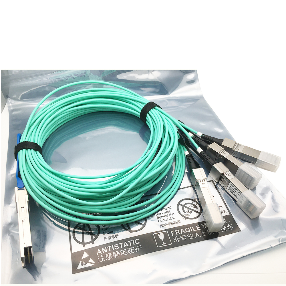
Overview of Cable Assembly

Order Information
P/N | Description |
Q4SFP+-AxxM | 40G QSFP+ to 4*SFP+ AOC Cable OM2/OM3/OM4, xx=0~100meter |
Logic | Symbol | Signal | Description | |
1 | GND | Signal Ground | Ground | |
2 | CML-I | Tx2n | Tx2n | Transmitter Inverted Date Input.AC coupled |
3 | CML-I | Tx2p | Tx2p | Transmitter Non_Inverted Date Input.AC coupled |
4 | GND | Signal Ground | Ground | |
5 | CML-I | Tx4n | Tx4n | Transmitter Inverted Date Input.AC coupled |
6 | CML-I | Tx4p | Tx4p | Transmitter Non_Inverted Date Input.AC coupled |
7 | GND | Signal Ground | Ground | |
8 | LVTTL-I | ModSelL | ModSelL | Module Select pin.Selected when held low by the host. |
9 | LVTTL-I | ResetL | LPMode_Reset | Module Reset.A"low" pulse induces a reset on the module. |
10 | Vcc Rx | Vcc Rx | +3.3V Power Supply Receiver | |
11 | LVCMOS-I/O | SCL | SCL | 2-wire serial interface |
12 | LVCMOS-I/O | SDA | SDA | |
13 | GND | Signal Ground | Ground | |
14 | CML-O | Rx3p | Rx3p | Receiver Non_Inverted Date Input.AC coupled |
15 | CML-O | Rx3n | Rx3n | Receiver Inverted Date Input.AC coupled |
16 | GND | Signal Ground | Ground | |
17 | CML-O | Rx1p | Rx1p | Receiver Non_Inverted Date Input.AC coupled |
18 | CML-O | Rx1n | Rx1n | Receiver Inverted Date Input.AC coupled |
19 | GND | Signal Ground | Ground | |
20 | GND | Signal Ground | Ground | |
21 | CML-O | Rx2n | Rx2n | Receiver Inverted Date Input.AC coupled |
22 | CML-O | Rx2p | Rx2p | Receiver Non_Inverted Date Input.AC coupled |
23 | GND | Signal Ground | Ground | |
24 | CML-O | Rx4n | Rx4n | Receiver Inverted Date Input.AC coupled |
25 | CML-O | Rx4p | Rx4p | Receiver Non_Inverted Date Input.AC coupled |
26 | GND | Signal Ground | Ground | |
27 | LVTTL-O | ModPrsL | ModPrsL | Module Present pin.Internally grounded inside the module. |
28 | LVTTL-O | IntL | IntL | Interrupt by the QSFP module."Low"indicates an Alarm/Warning. |
29 | Vcc Tx | Vcc Tx | +3.3V Power Supply Transmitter | |
30 | Vccl | Vccl | +3.3V Power Supply | |
31 | LVTTL-I | LPMode | LPMode | Low Power Mode |
32 | GND | Signal Ground | Ground | |
33 | CML-I | Tx3p | Tx3p | Transmitter Non_Inverted Date Input.AC coupled |
34 | CML-I | Tx3n | Tx3n | Transmitter Inverted Date Input.AC coupled |
35 | GND | Signal Ground | Ground | |
36 | CML-I | Tx1p | Tx1p | Transmitter Non_Inverted Date Input.AC coupled |
37 | CML-I | Tx1n | Tx1n | Transmitter Inverted Date Input.AC coupled |
38 | GND | Signal Ground | Ground | |
Housing | Chassis Ground |